Thickness Monitor
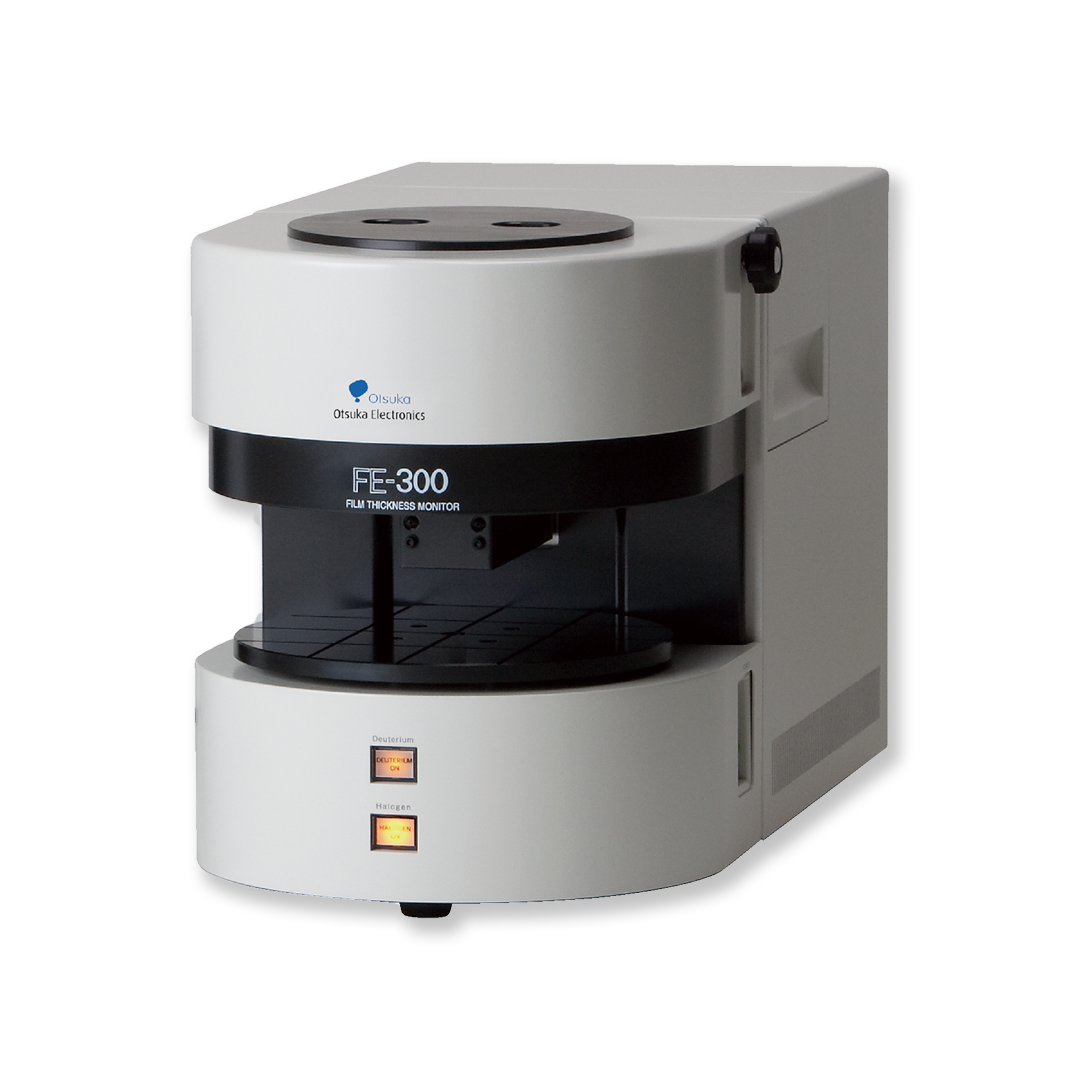
FE-300
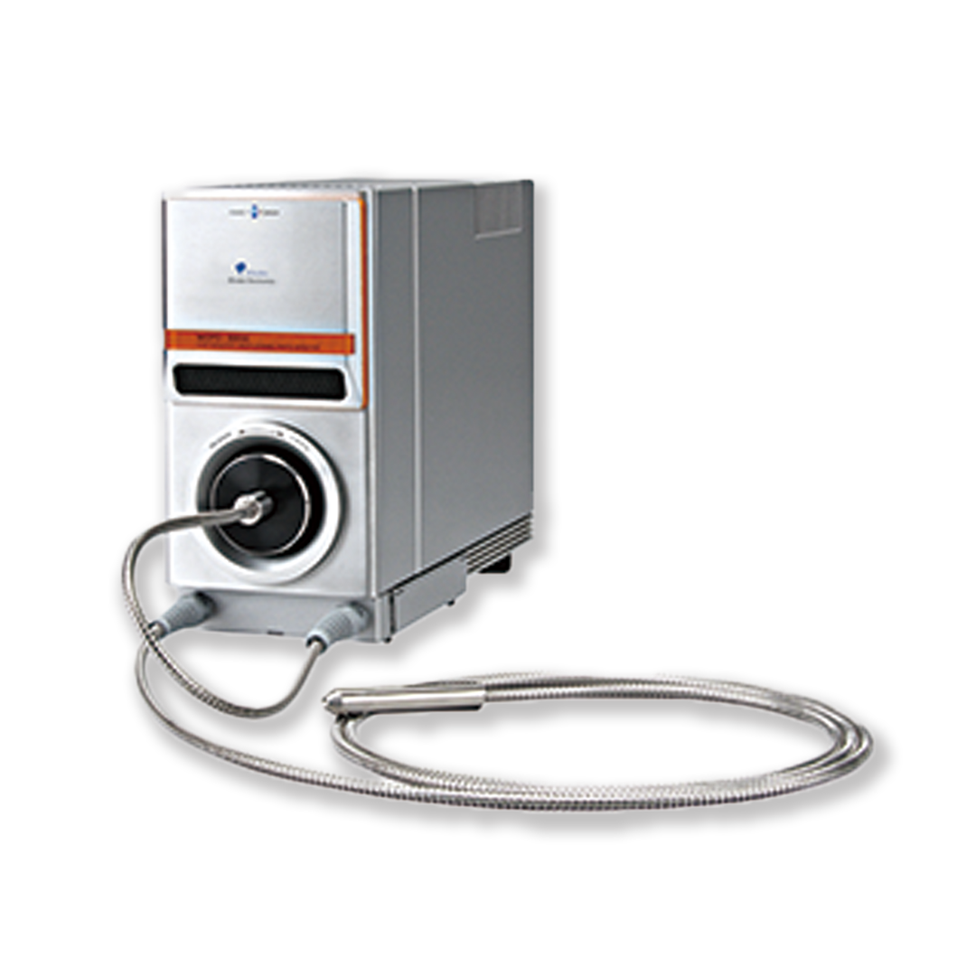
A film thickness measurement system based on the high precision spectrophotometry features compact size and affordable price. Every necessary component is built in one body for stable measurement data. Although offered at affordable price there is no compromise on accuracy and even optical constant analysis is possible.
- Function film, Plastic
- Semiconductor, Compound semiconductor
- Surface treatment
- Optical materia
- FPD
- Others
- Absolute reflectance
- Film thickness(Up to 10 layers)
- Optical constant(n: Refractive index, k: Extinction coefficient)
- Wide film thickness range (1nm~1mm)
- Thickness measurement using reflection spectrum
- Compact and affordable without compromising high precision
- User friendly software interface.
- Analytical algorisms are Peak-Valley Method, Fast Fourier Transformation (FFT) Method, Non-linear Least-Squares Method and Optimization Method.
- Optical constant analysis (n: Refractive index, k: Extinction coefficient) with Non-linear Least-Squares Method
Film Thickness Measurement Instrument About the Thickness Monitor FE-300
A film thickness measurement system based on the high precision spectrophotometry features compact size and affordable price. Every necessary component is built in one body for stable measurement data. Although offered at affordable price there is no compromise on accuracy and even optical constant analysis is possible.
Measurement Items
Absolute reflectance
Film thickness
(Up to 10 layers)
Optical constant
(n: Refractive index, k: Extinction coefficient)
Measurement Targets
Function film, Plastic
Semiconductor, Compound semiconductor
Surface treatment
Optical materia
FPD
Others
Principle / Configuration
Principle
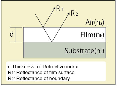
Otsuka Electronics provides non-contact and non-destructive thickness measurements with high accuracy using light interference method and own high performance spectrometer. Light interference method is the optical thickness analysis technique using the reflectance in the spectrophotometer optics. Given an example of the coated film on metal substrate, the beam irradiated from above reflects on the coating surface (R1).Also, transmitted beam reflects on the substrate or boundaries (R2). From the light interference behavior caused by optical path difference and phase shift, film thickness can be calculated using reflectance spectrum and refractive index. Analytical algorisms are Peak-Valley Method, Fast Fourier Transformation (FFT) Method, Non-linear Least-Squares Method and Optimization Method.
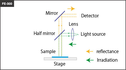
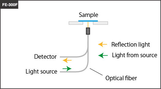
Configuration / Optics
Software
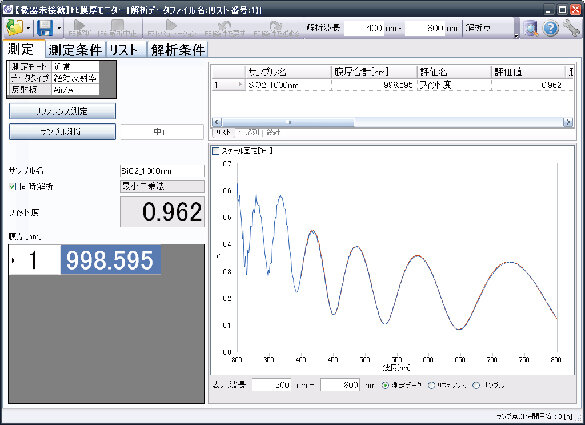
Measure Menu
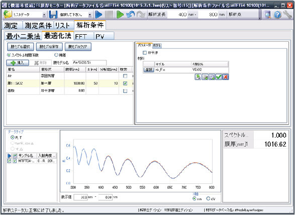
Analysis Condition Setting Menu
Measurement Examples
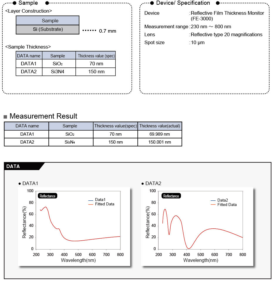
SiO2 SiN Thickness Measurement --- Application Sheet FE0002
The semiconductor transistor transmits signals by controlling the current conduction state. There is a built-in insulation film in between the transistors to prevent the current leakage and to avoid the accidental current inflow from another transistor. The insulation film is made of SiO2 or SiN. SiN has higher dielectric constant than SiO2 and can be used as a stopper to remove unnecessary SiO2 in CMP. To assess the efficiency as an insulation film and to keep the precise process management, it is mandatory to make a measurement of these film thicknesses.
Specifications
Measurement Examples
- Luminescence
- Luminous flux
- Goniophotometer
- Surface color measurement
- Reflectance
- Transmission / Absorbance
- Thickness
- Microscopic measurement
- Solution measurement
- Multi point measurement
- Production line
Contact
Please feel free to contact us with any inquiries or requests.
Related Product
Otsuka Electronics
Members Site
The Otsuka Electronics Members Site offers the following services.
We will continue to provide a wide range of content designed to enhance your professional knowledge and support your work.
Key Features of the
Members Site
-
Download product catalogs
-
Download technical documents
-
Watch member-only videos.
Feel free to reach out with any requests or questions.