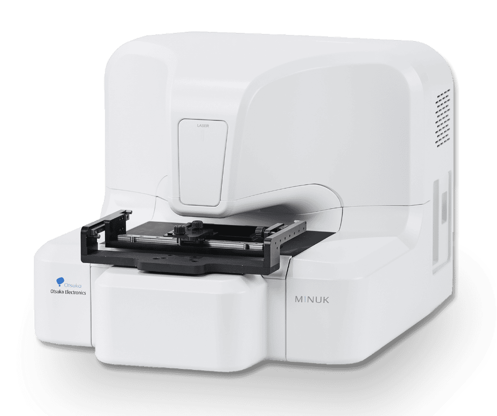
Three-Dimensional Optical Wave Field Microscope

See What Matters—Faster and More AccuratelyA Unique Microscopy Approach for Advanced Visualization and Quantification
Examples
Films
- Optical Waveguides
- Cells
- Glass
- Gels
- Protein Aggregates
Detection Targets
Scratches
- Voids
- Core Structures
- Fillers
- Cell Morphologies
- Refractive Index Variations
Observation Modes
OPD
- Bright Field
- Amplitude
- OPD Edge
- Edge
- Differential
Concept Behind the Development of MINUK
Conventional Approach
Seeing Through Lenses
Observing the world through lenses has long been the foundation of microscopy.
To obtain information as close to reality as possible, continuous advances in optics, image processing, computational analysis, and precision engineering have been pursued.
New Approach
Reveal the Invisible. Predict the Future.
Capture optical information directlyand compute how light waves propagate. Advanced high-speed computation visualizes the invisible, revealing the true nature of the target.
Challenges of Conventional Microscopes
- A limited field of view makes locating foreign particles and defects time-consuming.
- The inability to determine target depth requires repeated imaging to locate the area of interest.
- Invisible nanometer-scale changes remain difficult to detect.
WithMINUK,
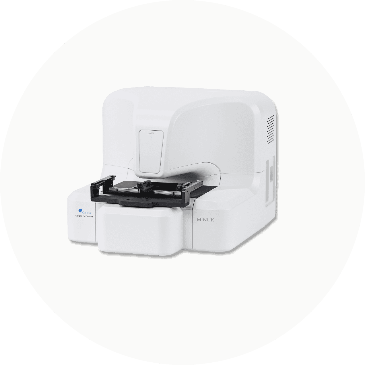
Place-and-Go 3D Imaging Non-Contact. Non-Destructive.No Physical Focusing Required. Observe and measure any point of interest, anytime.
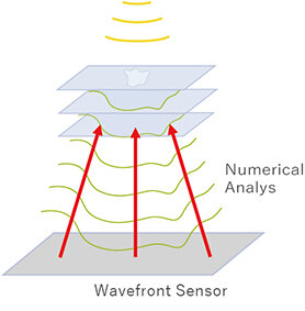
When a laser beam illuminates the target, variations in thickness and refractive index alter the optical wavefront. A wavefront sensor captures these changes, and our unique software uses advanced numerical analysis to reconstruct and visualize the object's internal structure.
Use Cases
Discover the Technical Challenges That Only MINUK Can Solve-
Challenge 1Want to distinguish particles from voids with high accuracy in film development?
Enables discrimination between particles and voids.OPD differences enable clear discrimination between particles and voids, supporting efficient defect root-cause analysis.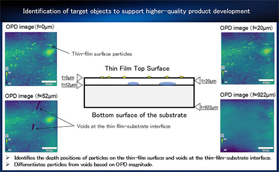
-
Challenge 2 Need to quantify hard-to-detect scratches to meet customer requirements for higher-quality product management.
Enables in-process nonconformance determinationEvaluate scratch height, cross-sectional shape, and 3D geometry to enable in-process defect identification.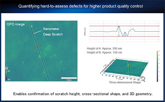
-
Challenge 3 Want to quantify whether the prototype geometry matches the design?
Enables precise quantitative measurement of inclined geometries.Provides reliable quantitative data and enables the quantification of film surface geometry.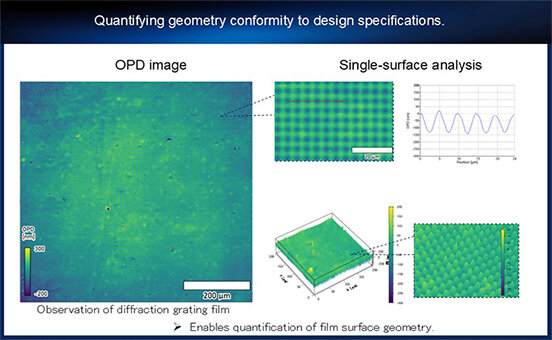
-
Challenge 4 Want to observe the core geometry of fibers and waveguides and quantify refractive index distributions?
Enables non-contact OPD observation.Enables easy, non-contact OPD observation, allowing optimization of condition studies without requiring significant time or effort.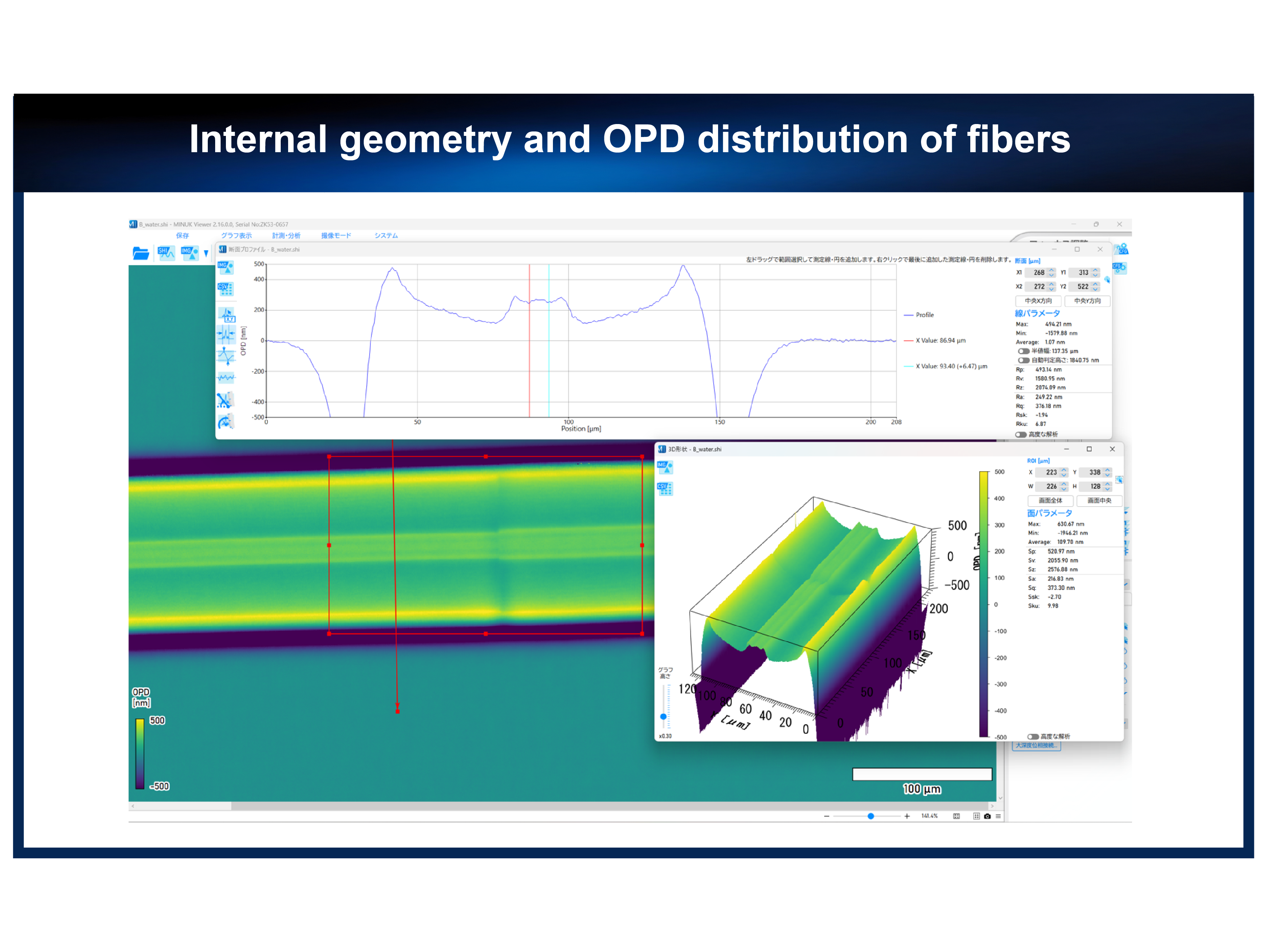
-
Challenge 5Want to quantify both the surface and internal geometry of TGVs and determine their depth positions?
Non-contact observation at arbitrary depthsEnables non-destructive observation of TGV geometry at any depth—from the glass surface through the interior to the back side—making it ideal for evaluating processing quality.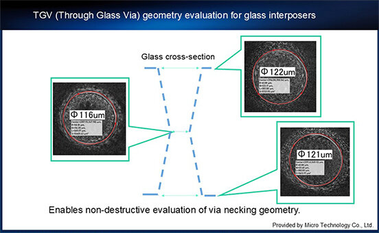
-
Challenge 6 Want to observe living organisms such as cells in their natural state, without staining or causing any damage?
Enable non-contact, non-invasive measurements.Enables non-contact, non-invasive measurement of cellular morphology and height, enabling evaluation using novel indicators.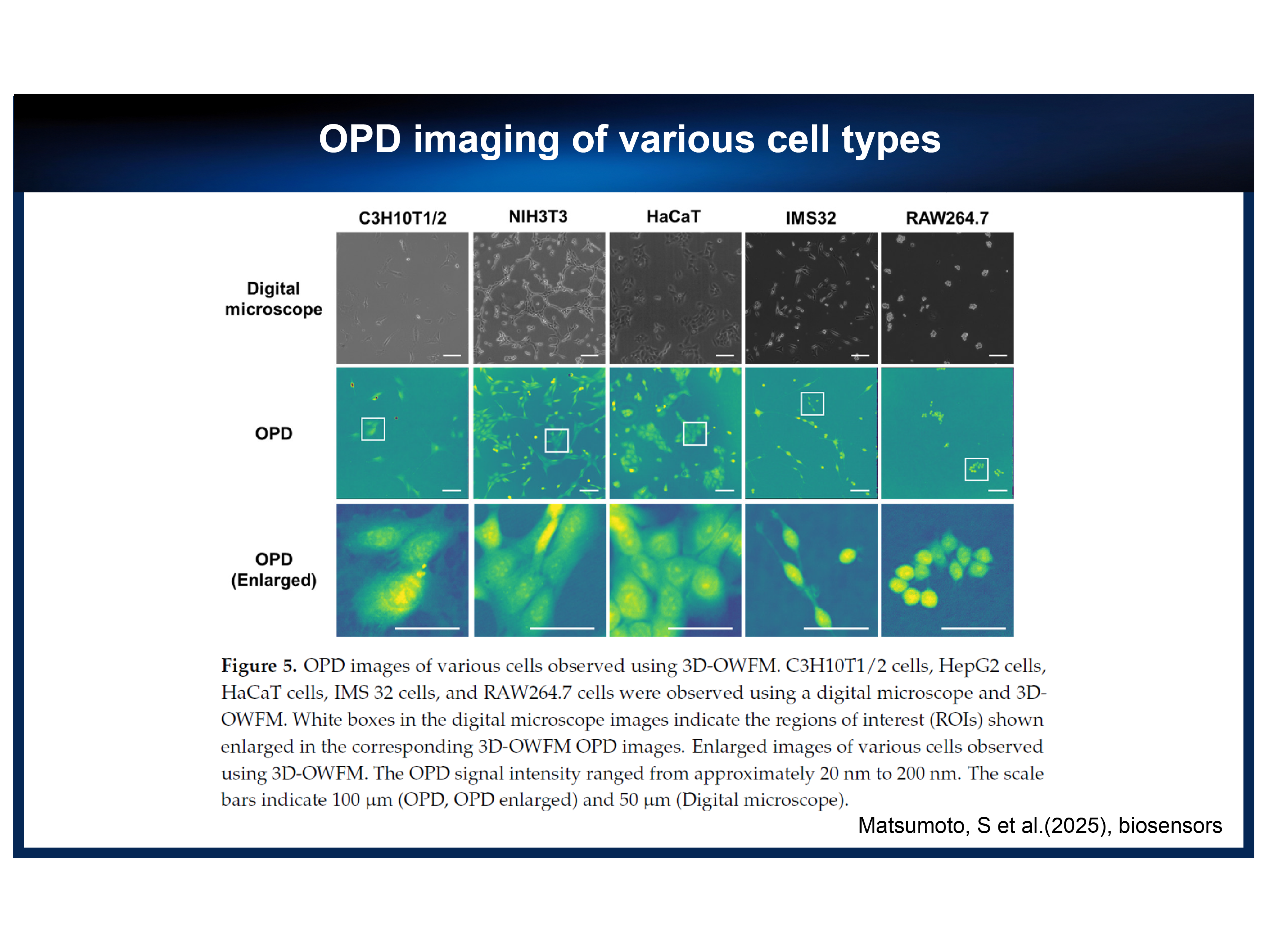
閉じる
Features
Quickly and easily measure the surface and internal features of transparent objects.-
Feature 01 Wide 700 μm field of view and high 488 nm resolution
With conventional systems, the narrow field of view often requires extensive searching to locate foreign particles and defects. MINUK overcomes this challenge by directly recording sample light without an imaging optical system,
Quickly locate foreign substances in the measurement target without the need for time-consuming searching.
fundamentally eliminating lens aberrations. The result is aberration-free imaging with a wide field of view and exceptional depth of field, making defect detection faster and more efficient.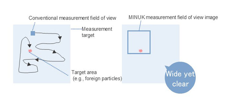
-
Feature 02 Capture complete information across a 1,400 μm depth range
Slice and visualize data at any desired depth. A single measurement captures information equivalent to thousands of images.Conventional systems require repeated image acquisition—sometimes thousands of images—because the depth of the target region is unknown. MINUK instantly captures information across a 700 × 700 μm field of view and a depth range of 1,400 μm. The acquired data yield approximately 700 slice images with a resolution of about 2 μm and can be digitally refocused for further verification of three-dimensional structures.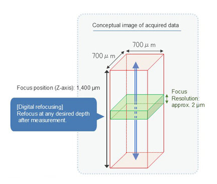
-
Feature 03 Visualize 3D distributions of transmittance and refractive index, and quantify invisible nanoscale surface geometry.
Conventional methods often made accurate focusing difficult, limiting quantitative analysis. MINUK overcomes these challenges by enabling quantification of invisible nanoscale surface geometry and detection of subtle refractive index variations.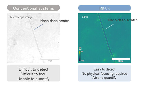
Video
Specifications
| Resolution (x, ý) | 691 nm (One Shot), 488 nm (Composition) |
|---|---|
| Field of view (x, ý) | 700 × 700 μm |
| Resolution (Z) | 10 nm (Retardation) |
| Field of view (Z) | ±700μm |
| Sample size | 100 × 80 × t20 mm (with Versatile Sample Holder) |
| Sample stage | Motorized fine XY stage X:±10mm Y:±10mm Coarse Stage X:129mm Y:85mm |
| Laser | Wavelength: 638 nm Output power: ≤ 0.39 mW, Class 1 (at the sample) |
| Dimensions (W × D × H): mm |
Main unit: 505 × 630 × 439 *PC and accessories not included. |
| Weight | 41kg |
| Power consumption | Main unit: 290 VA *PC and accessories not included. |
Contact
Please feel free to contact us with any inquiries or requests.
Otsuka Electronics
Members Site
The Otsuka Electronics Members Site offers the following services.
We will continue to provide a wide range of content designed to enhance your professional knowledge and support your work.
Key Features of the
Members Site
-
Download product catalogs
-
Download technical documents
-
Watch member-only videos.
Feel free to reach out with any requests or questions.