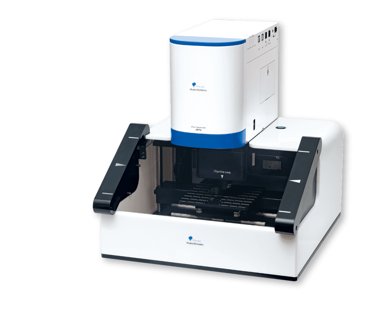
Optical Thickness Meter

Redefining Film Thickness Measurement!
Measure Virtually Any Film Type with a Single Instrument.
Measurement Applications
Semiconductors
- Films
- Solar Cells
- DLC
- FPD
- Optical Components
Measurement Examples
Oxide Films
- Nitride Films
- Photoresists
- AR Coatings
- Perovskite Films
- Various Optical Thin Films
Measurement Items
Absolute Reflectance
- Film Thickness Analysis
- Optical Constants Analysis (n: Refractive Index, k: Extinction Coefficient)
Concept Behind the Development of OPTM
Conventional Approach
Different film thickness measurement methods were required for different materials.
Dedicated film thickness measurement instruments were required depending on the sample transparency, color, and geometry.
New Approach
Enables film thickness measurements across a wide range of film types and sample geometries.
The OPTM Series easily measures a broad range of samples, from transparent to colored materials. With its micro-spot measurement capability, a single instrument can accommodate a variety of sample shapes and geometries.
Challenges of Conventional
Film Thickness
Measurement Instruments
- Different measurement targets require different instruments.
- Specialized knowledge is required for measurement and analysis.
- High-precision measurement is required for both thin and thick films.
With
OPTM Series,
Simpler, More Accurate Film Thickness MeasurementOne Instrument for Thin Films, Multilayer Films, and Diverse Measurement Challenges
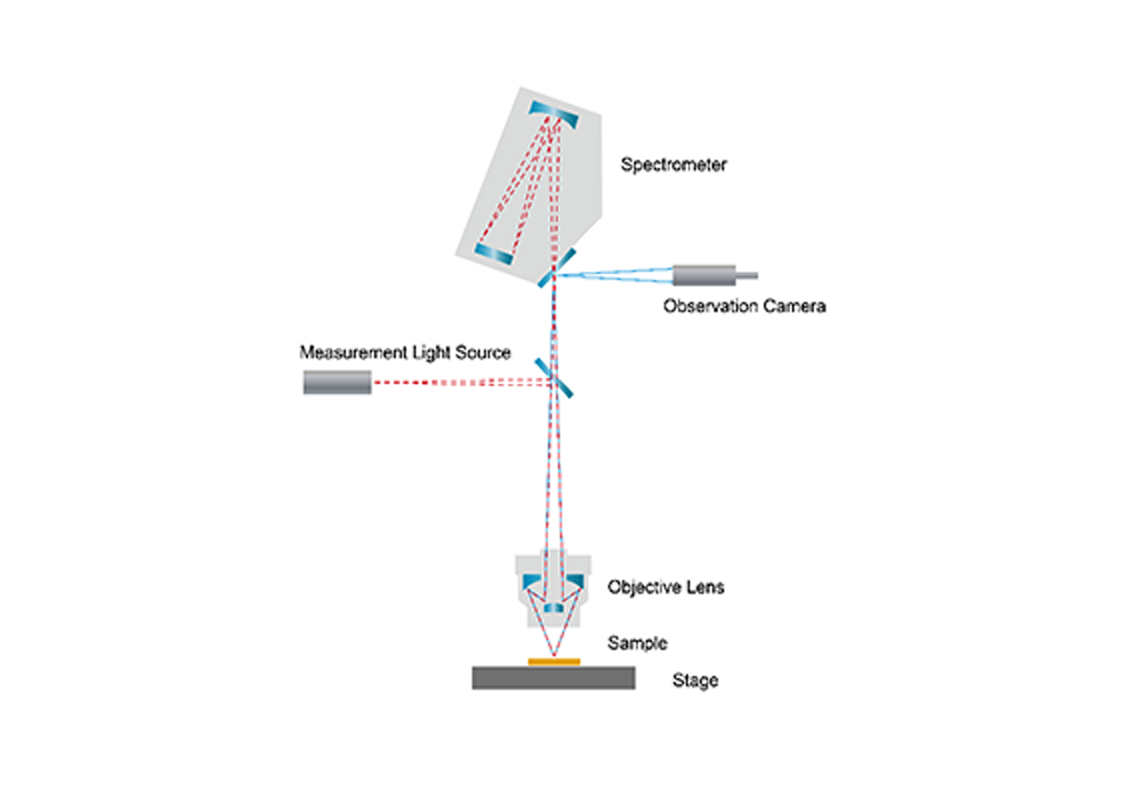
Microspectroscopy enables fast, non-contact, and non-destructive film thickness measurement in microscopic areas. By analyzing both film thickness and optical constants, the instrument supports a wide range of applications, from R&D to quality control.
Use Cases
Need a single film thickness meter for every location?-
Challenge 1Challenges in Measuring Thin and Multilayer Films
High-precision analysis of multilayer film thickness and optical constantsMeasure the thickness of each layer in perovskite solar cells with a single instrument. Non-contact, non-destructive measurement enables quick and easy analysis.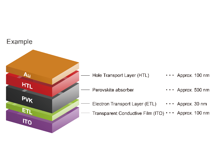
-
Challenge 2Need Fast Measurement of In-Plane Film Thickness Distribution
Non-Contact, Non-Destructive In-Plane Mapping MeasurementHigh-speed autofocus enables film thickness measurement at 25 points across a wafer in under one minute.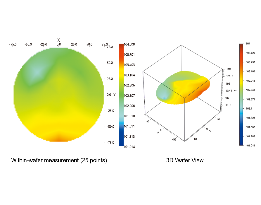
-
Challenge 3Challenges in Measuring Uneven or Stepped Surfaces
Supports measurement of wiring patterns with a micro-spot beam.With a minimum spot diameter of just 3 µm, measurements can be performed in ultra-small areas. In addition to TEOS/SiN/Si multilayer films, as shown in (1), the system can also measure patterned structures with 10 µm-wide trenches, as shown in (2).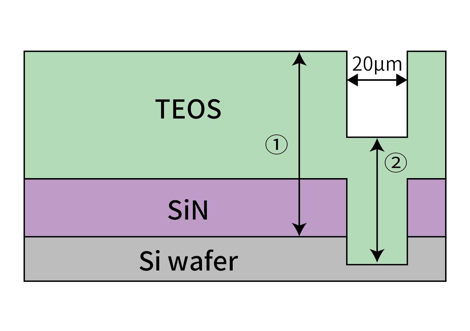
-
Challenge 4Thickness Analysis of Ultra-Thin Films Can Be Challenging
Accurate Optical Constants (n and k) Can Be Obtained Through Multi-Point Simultaneous AnalysisWhen the film thickness (d) is 100 nm or less, measurement accuracy may decrease, making it difficult to determine the exact value of d. In such cases, multiple samples with different film thicknesses are measured and analyzed simultaneously under the assumption that they share identical optical constants (n and k). This approach, known as multi-sample simultaneous analysis, enables more accurate determination of n and k, allowing the film thickness (d) to be determined more precisely.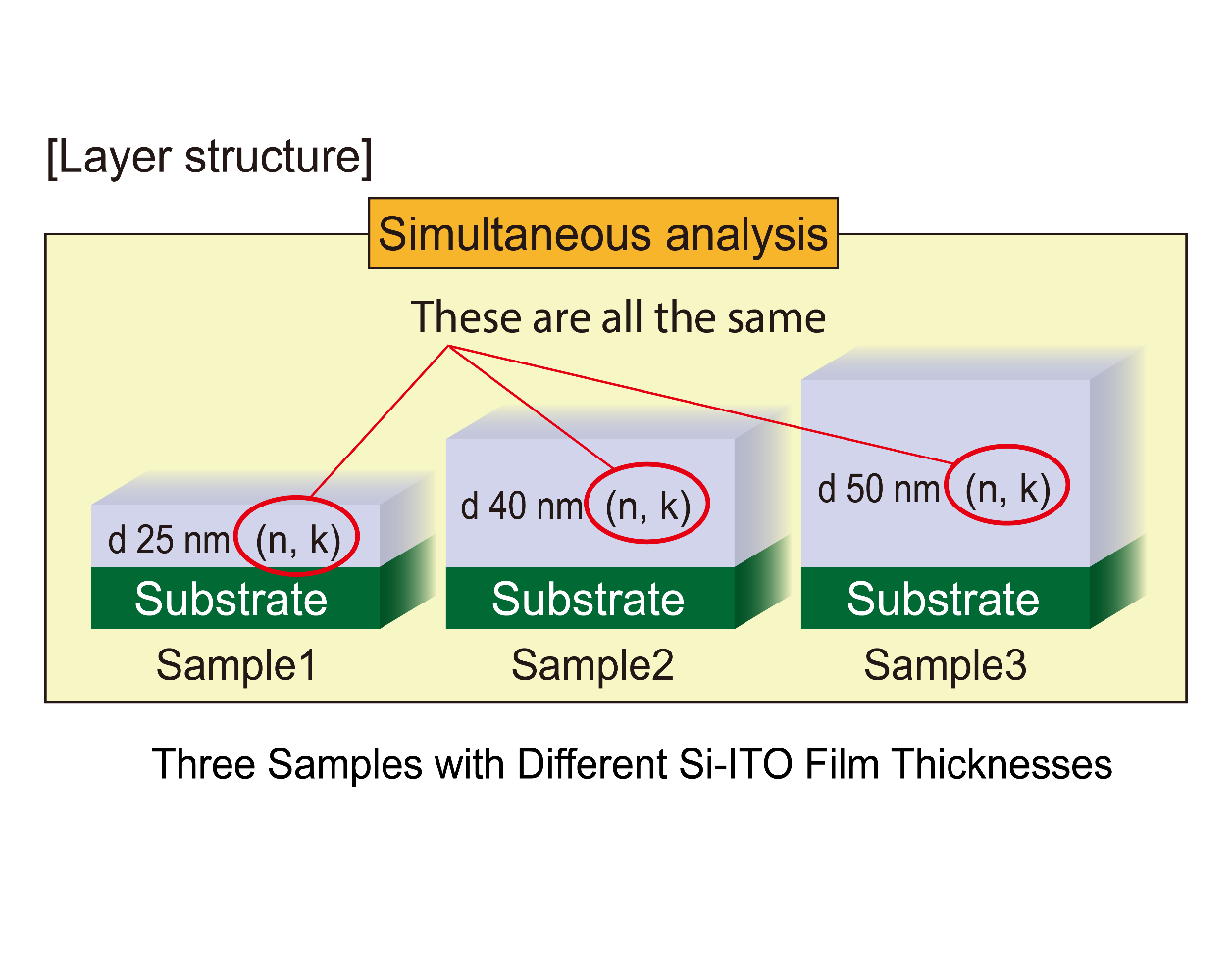
-
Challenge 5Need to Measure Small Areas on Complex-Shaped Samples
Micro-Optical System Enables Measurement of Extremely Small AreasEven on small and complex-shaped devices such as stents and balloon catheters, film thickness can be measured at specific locations. This enables verification based on actual measured values rather than estimates, providing more reliable and accurate thickness evaluation.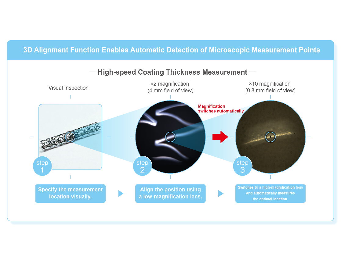
閉じる
Features
Solve All Your Film Thickness Measurement Instrument Challenges!-
Features 01 A Measurement Film That Goes Beyond Material Limitations
The OPTM Series uses spectroscopic measurement based on optical interferometry to enable highly accurate film thickness measurement regardless of film type. It accurately measures ultra-thin films, multilayer films, color filters, and transparent substrates that are traditionally difficult for conventional film thickness systems to measure. In addition, accurate absolute reflectance measurements enable analysis of a material's optical constants, including the refractive index (n) and extinction coefficient (k).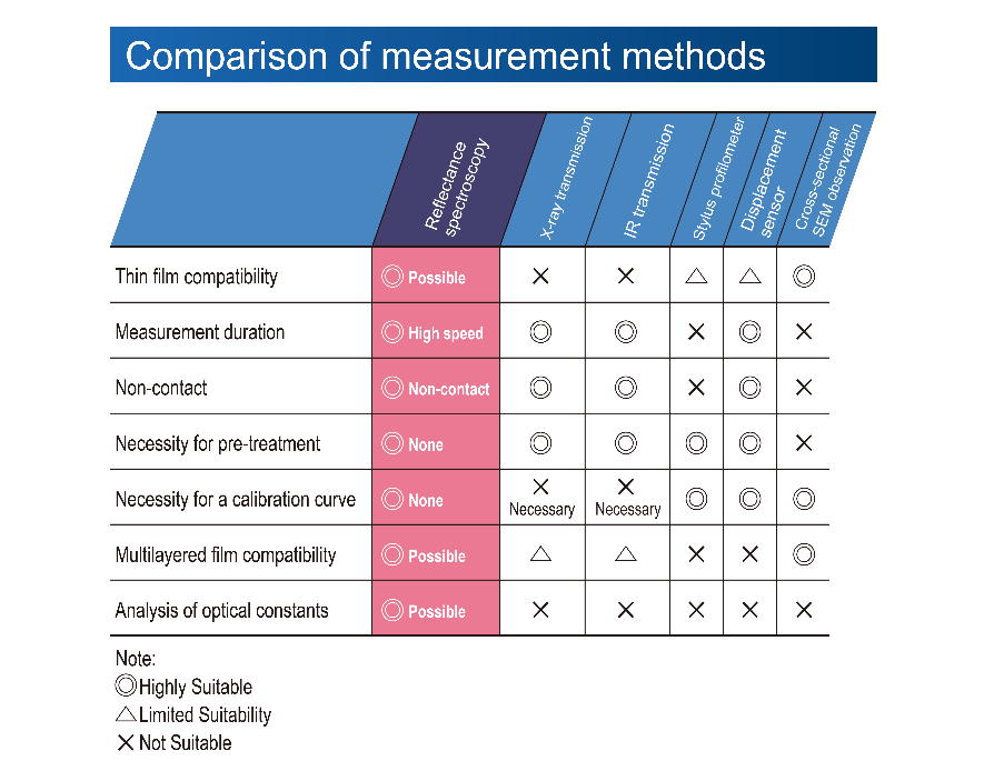
-
Features 02 Making Optical Constant Analysis More Accessible
Making Optical Constant Analysis More Accessible The OPTM Series features user-friendly functions that simplify film thickness measurement and optical constant analysis, enabling accurate measurements with ease for applications that previously required extensive experience and expertise.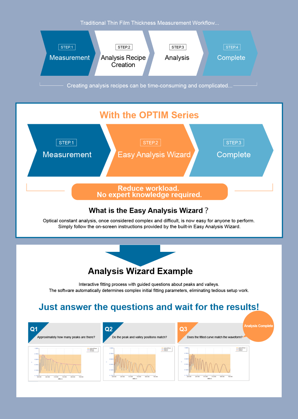
-
Features 03 Exceptional Inspection Speed and Accuracy
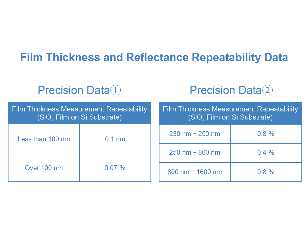
Thanks to high-speed AF (Auto Focus), measurements can be completed in as little as 1 second per point. With the OPTM-A1 Series equipped with an automated XY stage, up to 25 measurement points across a wafer can be measured in less than one minute. By employing a lens and optical system free from chromatic aberration, the OPTM series achieves:
- Film thickness repeatability of 0.1 nm
- Reflectance repeatability of 0.4% to 0.8%
-
Features 04 Additional Features
- Supports multilayer films of up to 50 layers
- Capable of measuring micro areas as small as 3 μm
- Equipped with an Area Sensor Safety System
- Includes various patented software technologies
- Customizable macro functions for a wide range of measurement sequences
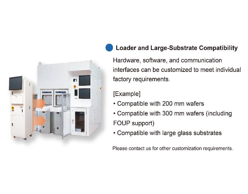
- Compatible with wafer loaders and large substrates
Specifications
| Type | OPTM-A1 | OPTM-A2 | OPTM-A3 |
|---|---|---|---|
| Wavelength Range | 230 nm to 800 nm | 360 nm to 1100 nm | 900 nm to 1600 nm |
| Film Thickness Measurement Range* | 1 nm to 35 μm | 7 nm to 49 μm | 16 nm to 92 μm |
| Sample Size** | Max.200 mm × 200 mm × 17 mm | ||
| Spot Size | Φ5, Φ10, Φ20, Φ40 | ||
For Automatic XY stage type
*Values are SiO2 equivalent thickness.
**Please contact us for consultation concerning the 300 mm stage.
| Type | Automatic XY stage type |
Fixed frame type | Built-in head type |
|---|---|---|---|
| Dimensions (W × D × H) | 556 × 566 × 618 mm | 368 × 468 × 491 mm | 210 × 441 × 474 mm 90 × 250 × 190 mm* |
| Weight | 66 kg | 38 kg | 23 kg 4 kg* |
| Maximum power consumption** | 500 VA | 400 VA | |
Contact
Please feel free to contact us with any inquiries or requests.
Otsuka Electronics
Members Site
The Otsuka Electronics Members Site offers the following services.
We will continue to provide a wide range of content designed to enhance your professional knowledge and support your work.
Key Features of the
Members Site
-
Download product catalogs
-
Download technical documents
-
Watch member-only videos.
Feel free to reach out with any requests or questions.