Si Wafer Thickness Monitoring System
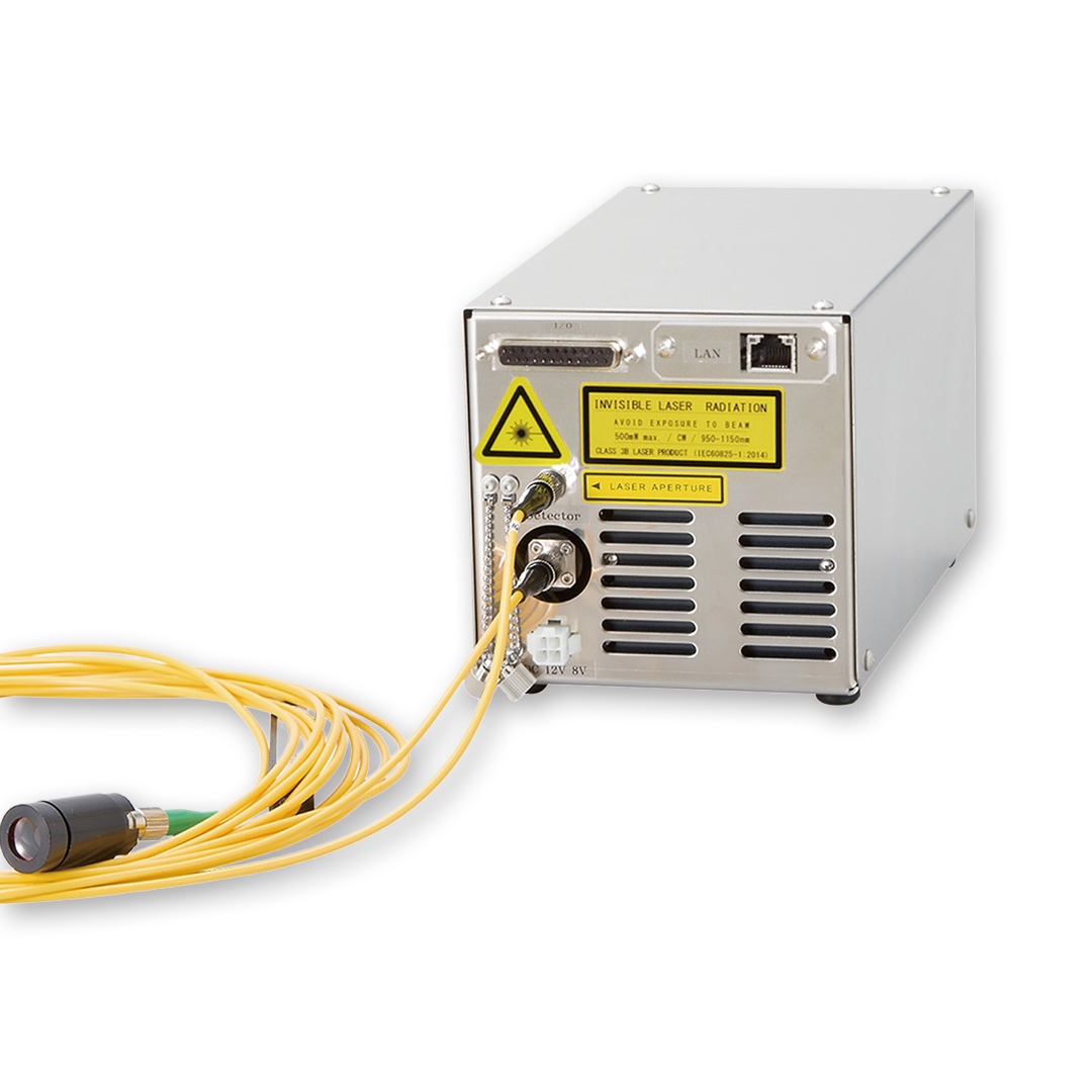
SF-3
Real-time measurement of Si wafer thickness at CMP or BG
Measurement Targets
- Thickness measurement for Si wafer material
- Grinding evaluation for silicon/ compound semiconductor
- 1.3 mm / next generation 450 mm wafer
- 775 ㎛ 300 mm wafer
- TSV wafer (Si layer thickness measurement on via)
- Other materials (SiO2, film)
Measurement Items
- Film thickness analysis (5 layers)
Features
- Non contact, non destructive measurement
- Parameter setting after spectrum analysis
- High speed real-time monitoring during CMP, BG
- Measurement over interlayer such as protection film and window material
- Multi layers analysis
- Original analytical engine (Patent pending)
- Original analytical algorism for thickness measurement (Patented)
- Automatic mapping function for thickness distribution
Film Thickness Measurement Instrument About the Si Wafer Thickness Monitoring System SF-3
Real-time measurement of Si wafer thickness at CMP or BG
Measurement Items
Film thickness analysis
(5 layers)
Measurement Targets
Specifications
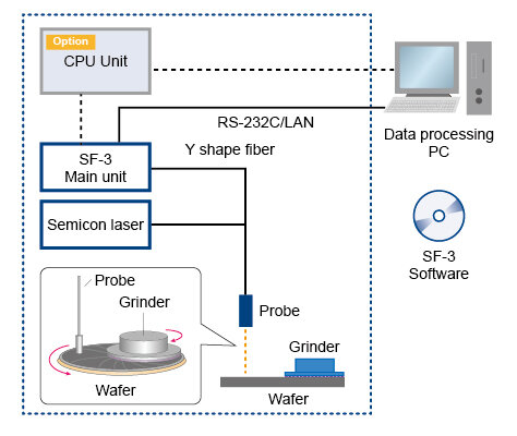
System Configuration
Contact
Please feel free to contact us with any inquiries or requests.
Otsuka Electronics
Members Site
The Otsuka Electronics Members Site offers the following services.
We will continue to provide a wide range of content designed to enhance your professional knowledge and support your work.
Key Features of the
Members Site
-
Download product catalogs
-
Download technical documents
-
Watch member-only videos.
Feel free to reach out with any requests or questions.