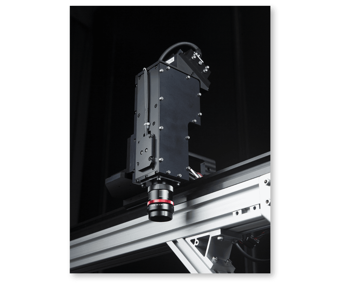
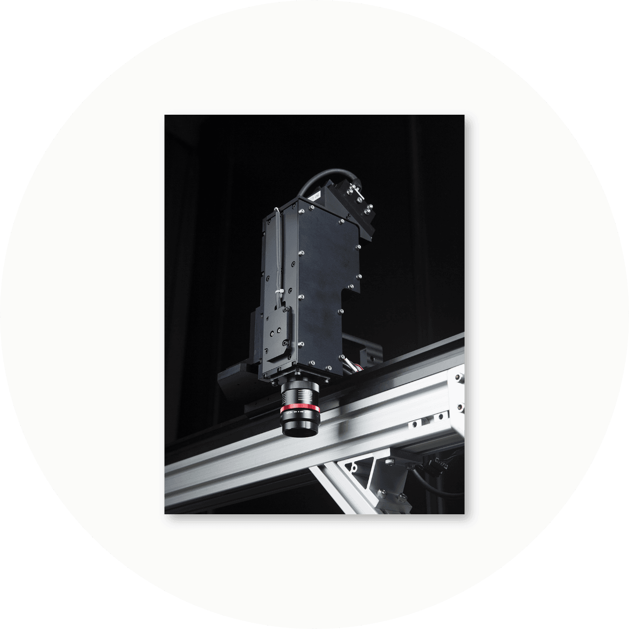
Line-Scan Thickness Monitor™

Calibration-Free Full-Width, Full-Length Film Thickness Measurement and Process Anomaly DetectionUses spectral interferometry instead of X-ray or infrared.
Measurement Object
Film Substrates
- Thin-Film Coatings on Films (AR, ITO, HC, etc.)
- Glass
- Functional Materials
- Medical Materials
Measurement Items
Film Thickness (2D Map, MD and TD Trends)
Examples of Detectable Defects
MD Streaks
- Cross-Web Bands
- Diagonal Non-Uniformities
- Chuck Marks
- Spot Defects
Concept Behind the Development of
Line-Scan Thickness Monitor™
Conventional Approach
Determine product quality by measuring only specific locations on the product.
Inline measurement typically relied on spot measurements, making it difficult to assess the quality of the entire product surface.
New Perspective
Ensure product quality by measuring the entire width and length of the product.
Line-Scan Thickness Monitor™ measures film thickness across the full width and entire length of the film, enabling quality assurance based on actual measurement data. In addition, it contributes to improved yield by detecting process anomalies and early warning signs, and providing feedback for corrective action.
Challenges of Conventional
Inline Thickness Monitors
- Customers and end users are demanding stricter film thickness control.
- Need to detect film thickness anomalies across the full width and entire length of the film without any detection gaps.
- Film flutter prevents accurate and stable measurement.
With
Line-Scan
Thickness Monitor™
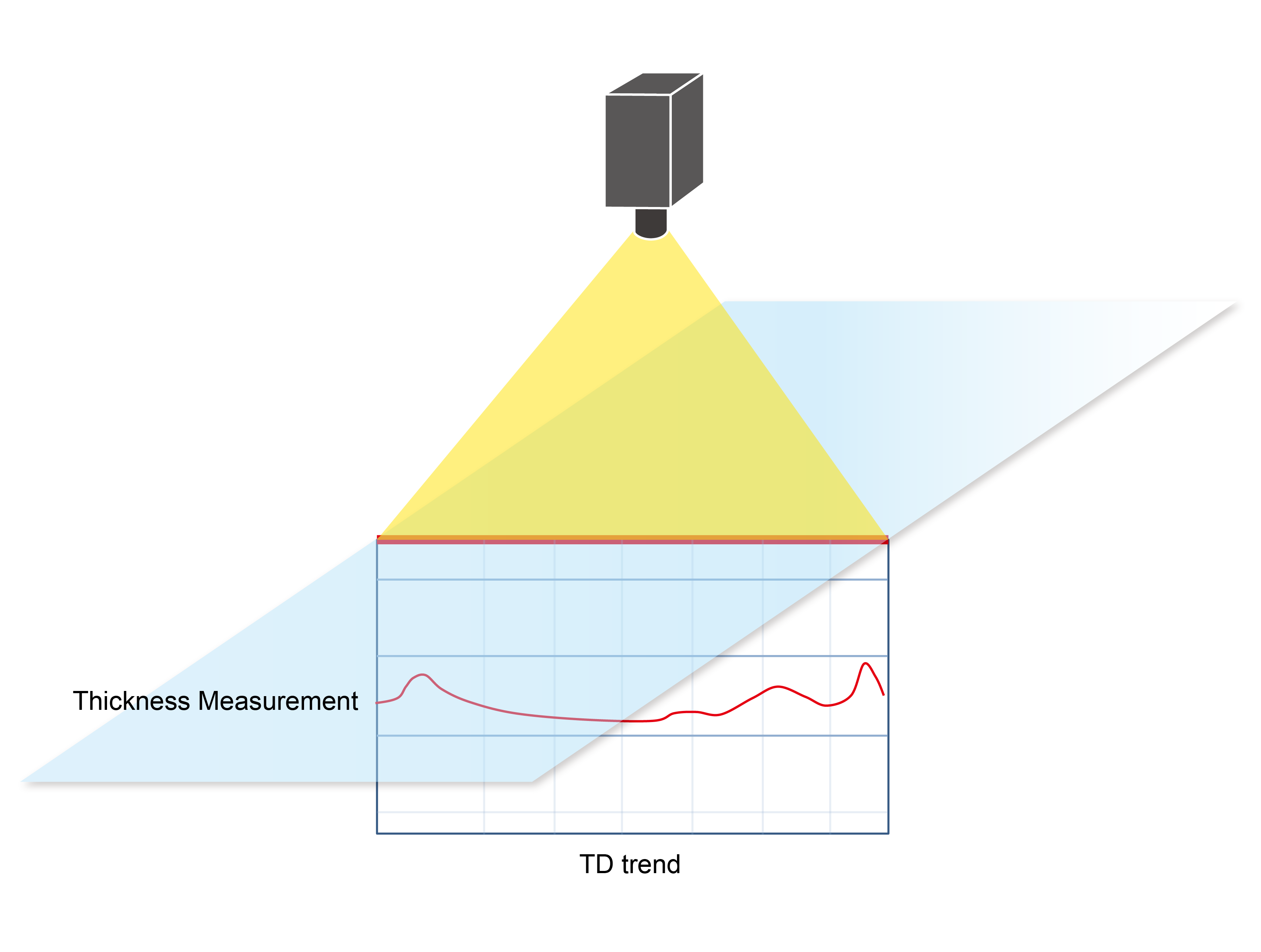
Full-width and full-length measurement enables visualization of previously undetectable thickness variations.A comprehensive view of thickness distribution is provided through contour maps and TD/MD trend displays.
Visualize thickness variations that are undetectable with spot measurements and leverage the results for quality assurance and process control.
Use Cases
Discover the Technical Challenges That OnlyLine-Scan Thickness Monitor™ Can Solve
-
Challenge 1 Need to meet increasingly stringent quality requirements.
Achieve quality assurance based on actual measurement data obtained through full-width and full-length measurement.Enables visualization of thickness distribution.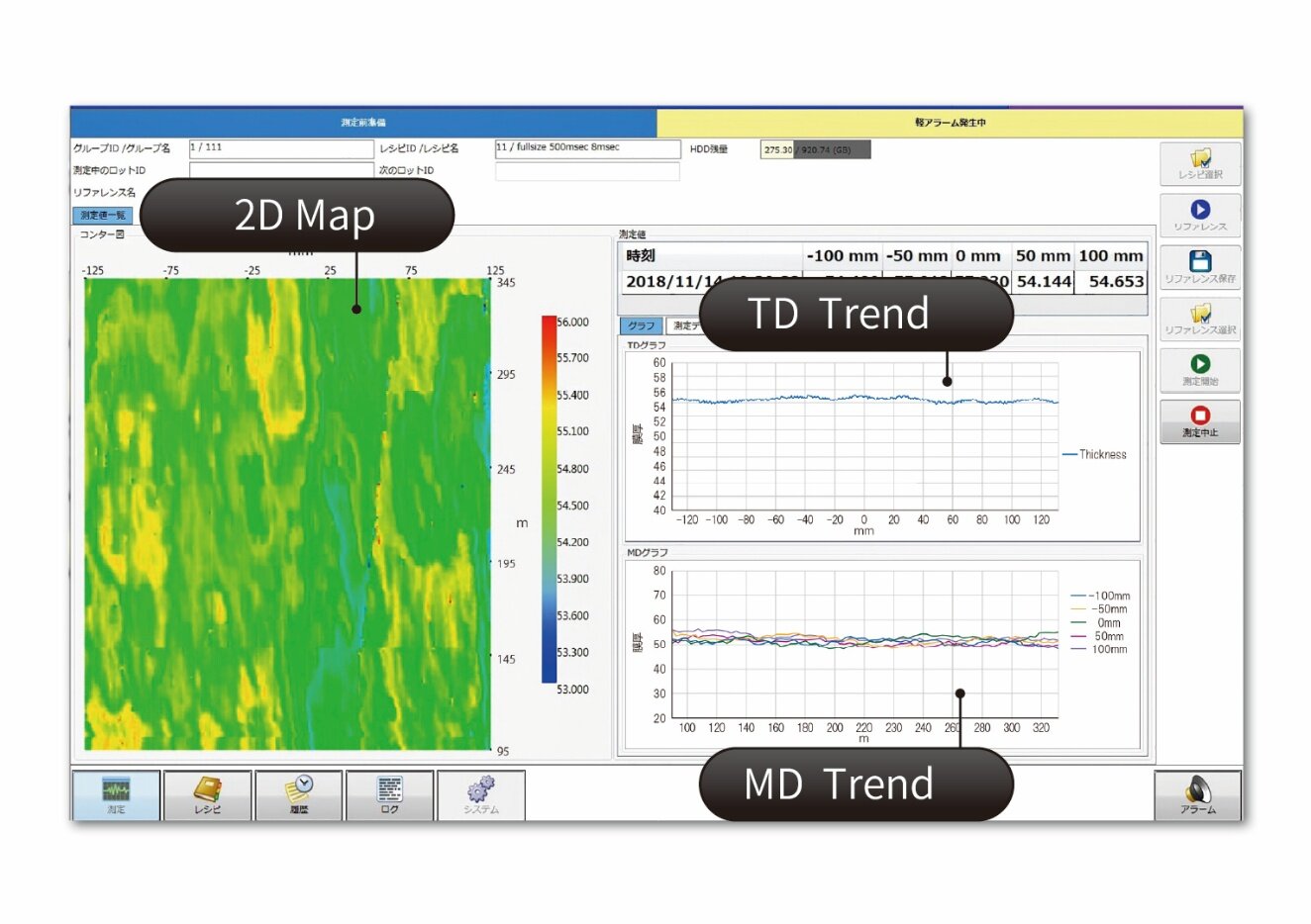
-
Challenge 2Time-consuming root cause analysis when anomalies occur.
Enable anomaly detection during the process.Enables identification of the location of anomalies in both the MD and TD directions.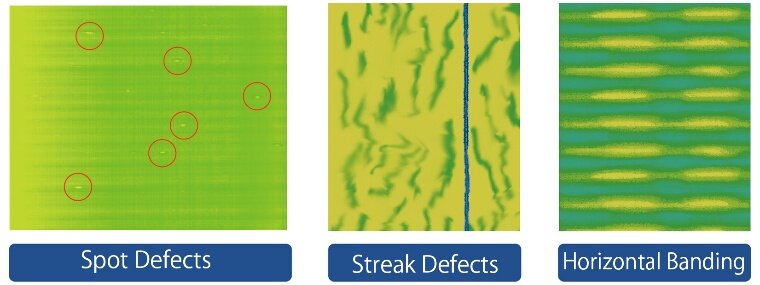
-
Challenge 3Need to efficiently handle wide samples.
Supports widths of up to 10 m and enables centralized management.By installing multiple cameras in the TD direction, measurement across the full width is possible without any gaps.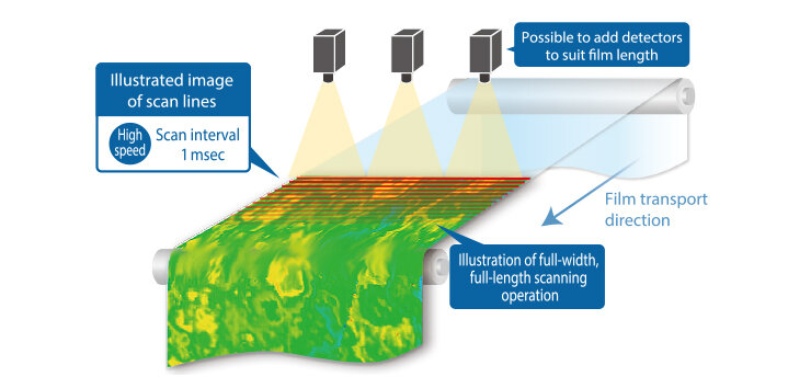
-
Challenge 4Need to measure without reducing line speed.
Enables high-speed measurement at intervals down to 1 ms.Enables detection of spot defects down to 1 mm without altering production conditions.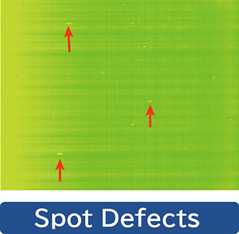
-
Challenge 5 Difficulty in achieving stable measurements due to film flutter.
Minimizes the effects of film flutter through a proprietary optical system.Stable measurements enabled by a proprietary optical system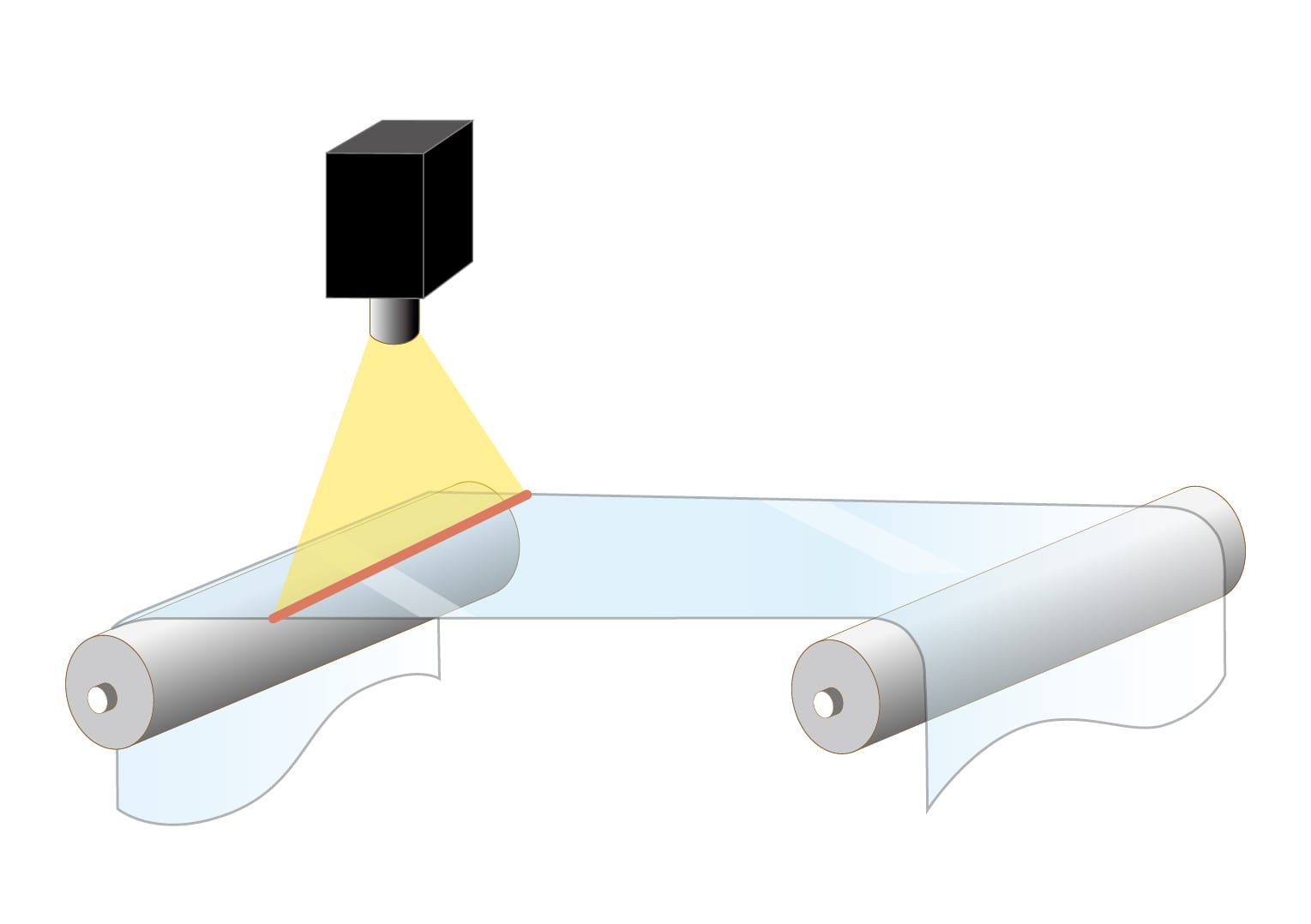
閉じる
Features
Line-scan technology enables complete film inspection with no inspection gaps.-
Feature 01 Enables high-resolution measurement with 1 mm spatial resolution in the MD and TD directions.
Conventional spot measurements often leave significant gaps in data coverage across the full width and length of the film. With high spatial resolution and measurement intervals as short as 1 ms, Line-Scan Thickness Monitor™ enables full-width and full-length measurement, supporting both quality assurance and process anomaly detection. -
Feature 02 Wide thickness measurement range from 0.1 to 300 μm.
Thanks to its wide measurement range, a single system can measure the thickness distribution of both film substrates and coatings. -
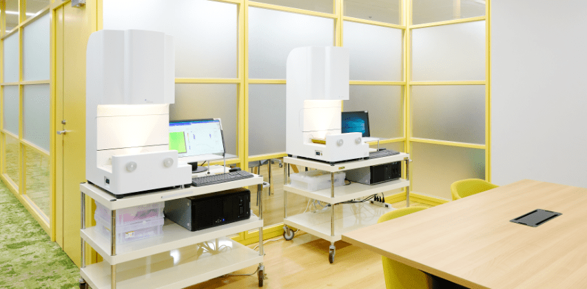
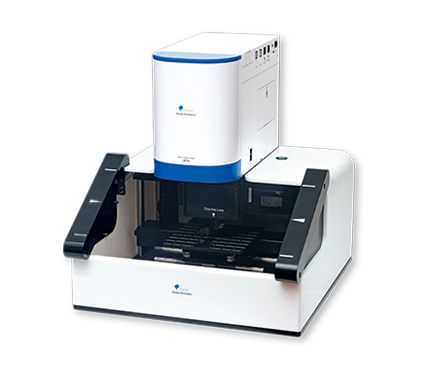
Feature 03 Offline models are also available for quality control applications.
Suitable for R&D and quality control applications.
Measures the thickness distribution of cut samples up to 250 mm wide in less than a minute.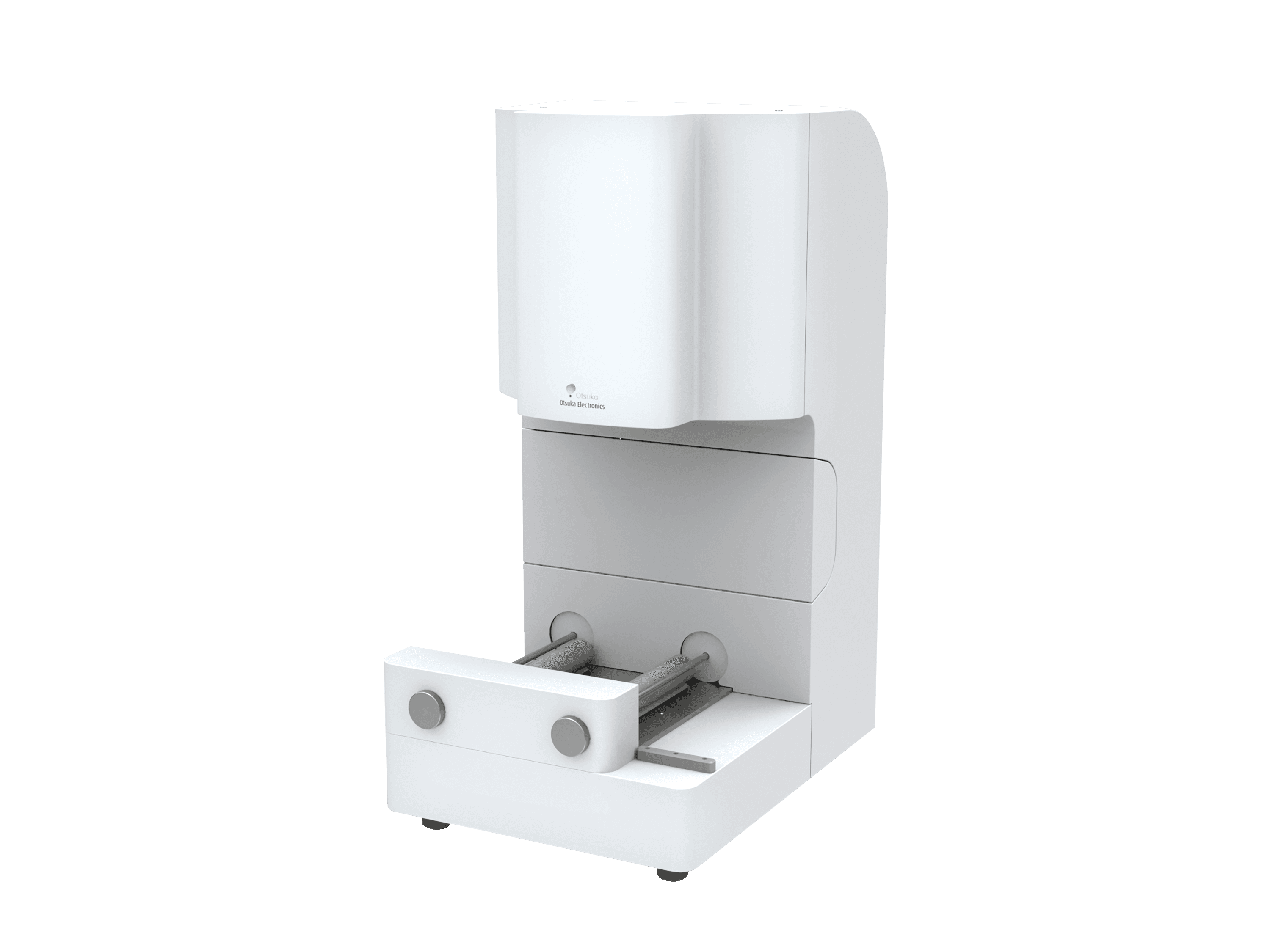
Specifications
| Measurement Items | Film thickness(FFT) |
|---|---|
| Spatial resolution | 1 mm |
| Transverse width | 500 mm |
| Wavelength width per element | Approx. 0.6 nm |
| Film thickness range | 2 to 300 μm |
| Scan interval | 10 msec or larger |
Contact
Please feel free to contact us with any inquiries or requests.
Otsuka Electronics
Members Site
The Otsuka Electronics Members Site offers the following services.
We will continue to provide a wide range of content designed to enhance your professional knowledge and support your work.
Key Features of the
Members Site
-
Download product catalogs
-
Download technical documents
-
Watch member-only videos.
Feel free to reach out with any requests or questions.